multicore-5-stage-cpu
Design, Verification and Synthesis of a 5-Stage Pipelined Multicore CPU on Altera DE2-115 (>50MHz)
This project implements a dual-core pipelined processor with a snoopy-bus and split caches, provides functionally verified modules and thoroughly tests for edge cases in protocols. All source files and tcl scripts for this project can be found here. This project was completed as a part of ECE 437, and requires that code be private – Please reach out if you’d like to view it, and are not taking the course.
Below, I’ve formatted our Final Report (that got us an A) for the site, but want to quickly highlight that the core is tested on these custom testbenches:
- Fibonacci Sequence
- Linear Search
- Insertion Sort and Merge Sort
- Booth’s Encoding Multiplication
- Number of Days between Dates
- Producer-Consumer-based Recursive CRC ChkSum
Overview
This report presents a comparison of four variants of our RISC-V processor design: the single-cycle processor, the 5- stage pipeline without caches, the pipeline with a two-level cache hierarchy, and the multicore processor. All designs execute instructions based on the same subset of the RISC Instruc- tion Set Architecture (ISA), but incrementally build on each other to replicate previous- generation CPUs, leading to differences in clock speed and hardware complexity.
All designs execute the same mergesort benchmark (and, where necessary, the dual.mergesort variant) to ensure a fair comparison. The single-cycle processor executes a single instruction per clock cycle, leading to a straightforward design. However, since it is required to complete the multiple aspects of an instruction within a cycle, it leads to low clock speeds. On the other hand, the pipelined processor splits up part of the instruction execution into different stages, ensuring that each stage completes in a single cycle. The pipelined version without caches exposes the full memory-access latency while the cached pipeline hides much of it at the cost of added hard- ware. On the other hand, the multicore design allows for parallel speedup, but at suffers some coherence overhead. We expect the cached pipeline to outperform the uncached ver- sion as memory latency increases, and the multicore design to show greater speedup on the dual-threaded mergesort.
To confirm our above expectations, we compare each design in the FPGA flow to collect synthesis frequency, average CPI, total execution time (for different memory access latencies), instruction latency, and resource utilization. Section 2 details the architectural diagrams and state machines for the pipeline, caches, and coherence logic; Section 3 presents the full performance and resource-utilization results; Section 4 discusses conclusions drawn from these data; and Section 5 documents individual contributions.
Below, we provide the Instruction-type breakdowns for each benchmark used. Note that these breakdowns are generated post-simulation, and will show variance between Core 0 and Core 1 counts due to real-life multi-core coherence overhead. We will use these numbers while calculating the CPI for our designs.
| Instruction Type | Count | Percentage |
|---|---|---|
| R‑Type | 823 | 15.22% |
| I‑Type | 834 | 15.42% |
| LW | 806 | 14.90% |
| SW | 691 | 12.77% |
| JAL/JALR | 695 | 12.85% |
| B‑Type | 1560 | 28.83% |
| TOTAL | 5409 | 100% |
| Instruction Type | Core 0 Count | Core 0 Percentage | Core 1 Count | Core 1 Percentage |
|---|---|---|---|---|
| SLL | 2 | 0.06% | 2 | 0.09% |
| SRL | 2 | 0.06% | 1 | 0.04% |
| SLT | 378 | 11.91% | 300 | 13.30% |
| SLTU | 32 | 1.01% | 32 | 1.42% |
| SUB | 3 | 0.09% | 3 | 0.13% |
| ADD | 34 | 1.07% | 32 | 1.42% |
| OR | 8 | 0.25% | 0 | 0.00% |
| ORI | 11 | 0.35% | 9 | 0.40% |
| LW | 476 | 15.00% | 332 | 14.72% |
| SW | 389 | 12.26% | 303 | 13.43% |
| BEQ | 863 | 27.19% | 634 | 28.10% |
| BNE | 64 | 2.02% | 0 | 0.00% |
| ADDI | 518 | 16.32% | 302 | 13.39% |
| JAL | 389 | 12.26% | 303 | 13.43% |
| JALR | 2 | 0.06% | 1 | 0.04% |
| LUI | 2 | 0.06% | 1 | 0.04% |
| TOTAL | 3173 | 100% | 2256 | 100% |
Architecture
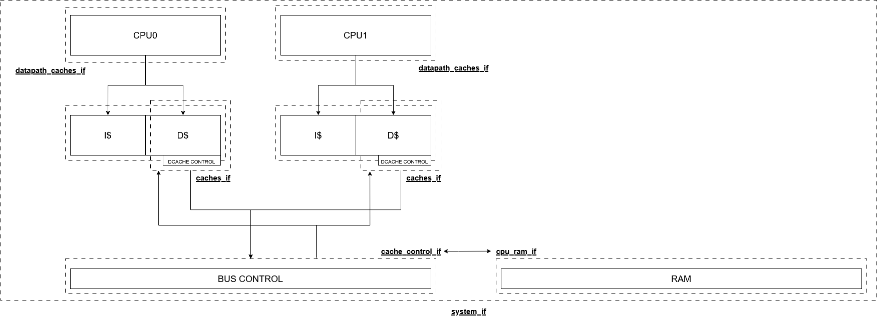
Figure 1 highlights the top-level block diagram of the interfaces we use throughout our design variants. The Caches block is a pass-through for the standalone singlecycle/pipeline, and contains some basic combinational logic to highlight completion of memory requests. The Datapath block contains the main processor implementation through which the instructions flow.

Figure 2 visualizes the single-cycle processor design.
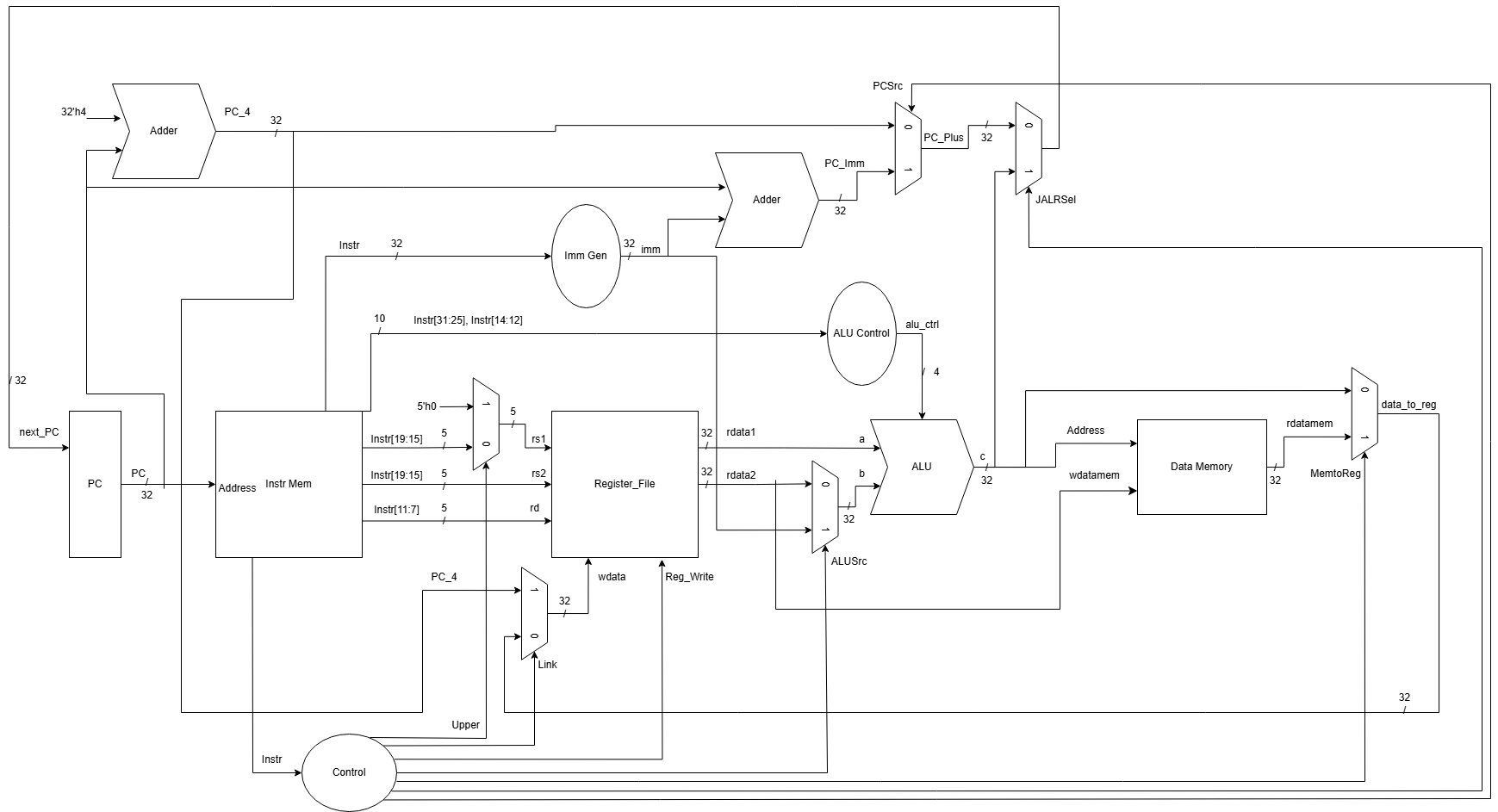
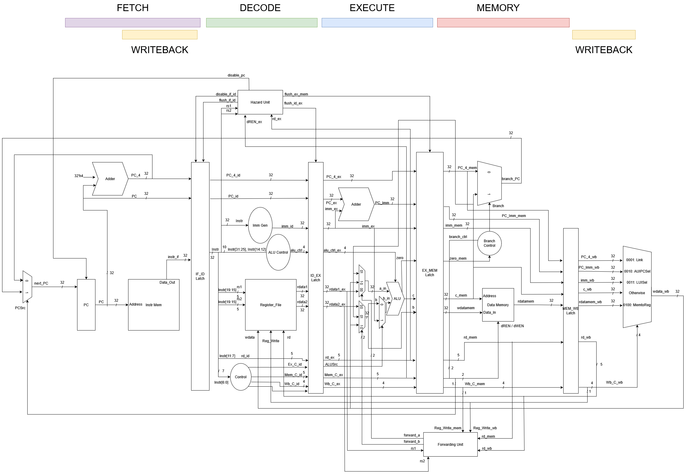
Figure 3 outlines our pipelined processor design. Here, every memory access in the Memory stage must wait for main-memory latency, leading to pipeline stalls whenever an instruction issues a load or store. Forwarding and Hazard modules (within Datapath) are responsible for ensuring minimal bubble additions while resolving data and control hazards.
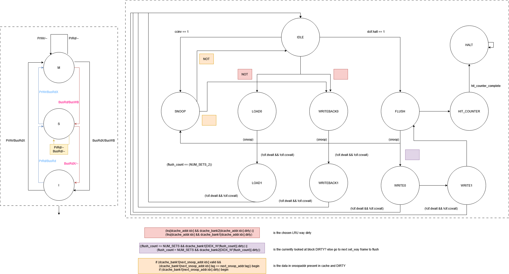
In the cached pipeline (Figure 4), we added a split L1 hierarchy: a direct-mapped instruction cache, and a 2-way set-associative data cache. The number of frames and index-splits of the addresses are parameterizable. Each cache uses a write-back, write-allocate policy. On an L1 miss, the data cache controller initiates either LOAD or WRITE-BACK FSM over the simple bus controller and stalls only the Memory stage, allowing earlier stages to continue if they do not depend on the miss. The instruction cache does not allow for writing, but contains an FSM to load the instructions on a miss.
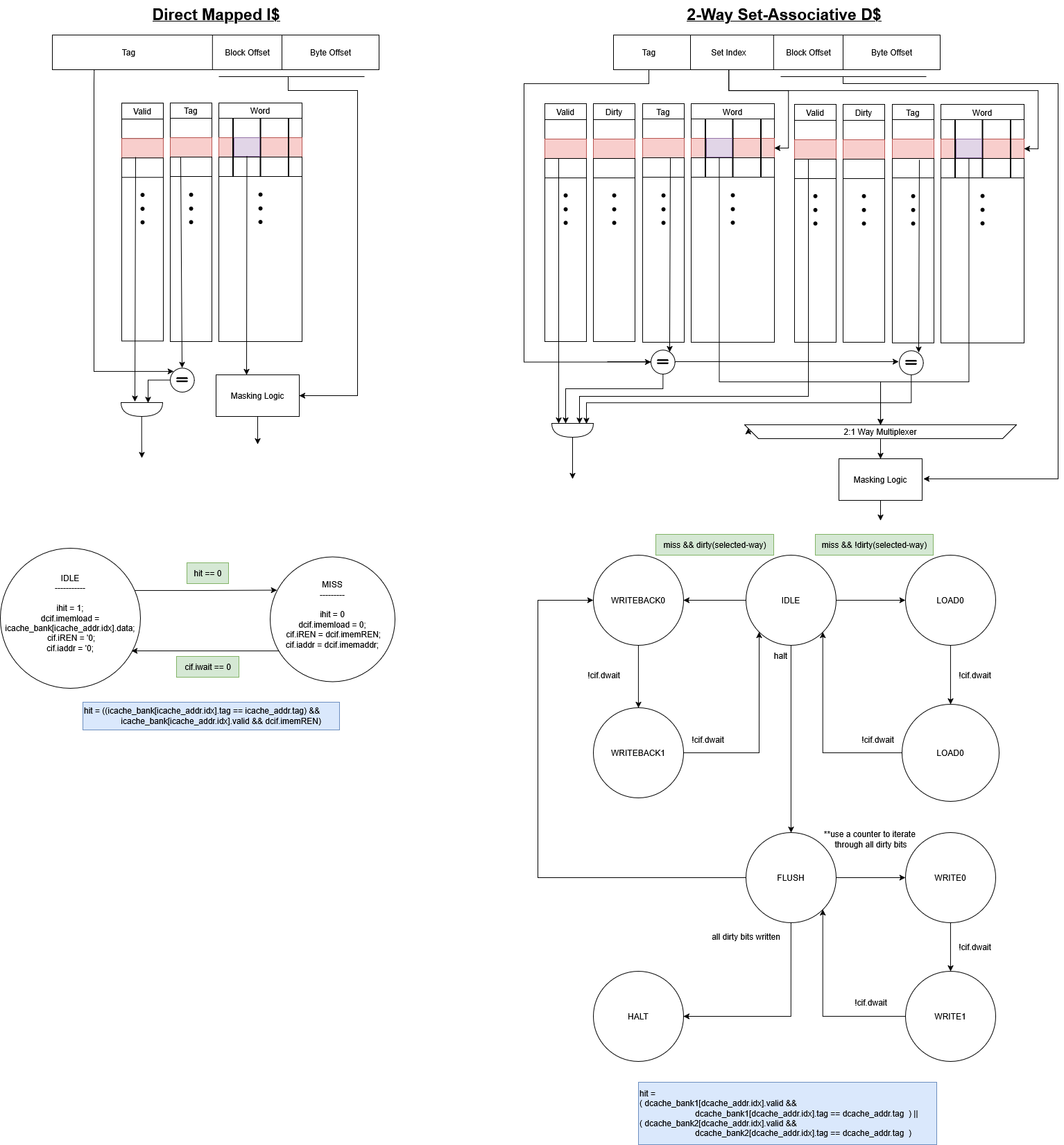
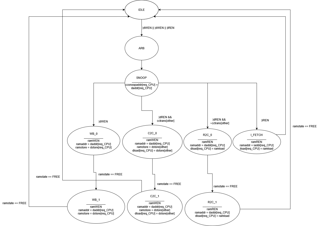
Our multicore design (Figure 5) instantiates two identical pipelined datapaths, highlighted as CPU0 and CPU1, each with its own split L1 caches, connected to a shared Bus Control module. We implement the MSI coherence protocol, with no additional SRAM arrays to coordinate the states of each frame. The Bus Controller’s state diagram in Figure 6 arbitrates between competing requests and broadcasts snoop responses. Each core’s data cache includes additional logic to support LR/SC atomic operations, modeled after the RISC-V specification, as shown in Figure 7.
Results
In this section, we compare the aforementioned designs based on performance metrics such as frequency, cycles per instruction (CPI), instruction latency, total execution time, and FPGA resource utilization. Below, we outline the formulas used to calculate each metric, a short paragraph targeting specific requirements, followed by tables presenting our overall results for all designs.
Maximum Clock Frequency
The maximum clock frequency is extracted from the system.log report.
\[f_{\text{max}} = \min\left(\frac{\text{CLK}}{2}, \text{CPUCLK} \right)\]For the pipelined, non-cache processor, \(f_{\text{max}} = 65.23 MHz\)
For the pipelined, processor with cache, \(f_{\text{max}} = 55.85 MHz\)
For the final multicore processor, \(f_{\text{max}} = 50.04 MHz\)
Average Cycles per Instruction (CPI)
CPI is calculated as:
\[\text{CPI} = \frac{\text{Total Clock Cycles}}{\text{Total Instructions Executed}}\]where:
- Total Clock Cycles is obtained from the make system.sim command.
- Total Instructions Executed is reported at the end of the simulation (sim -t or sim -t -m).
NOTE: The Total Instruction count for mergesort is 5409 and dual.mergesort and 5429.
Total Execution Time
The total execution time for the program is given by:
\[\text{Total Execution Time} = \frac{\text{Total Clock Cycles}}{f_{\text{max}}} s\]Instruction Latency
Instruction latency represents the time taken for a single instruction to complete.
\[\text{Latency}_{\text{single-cycle}} = \frac{\text{Execution Time}}{\text{Total Instructions Executed}} s\]FPGA Resource Utilization
The FPGA resource usage includes:
- Total Logic Elements – Represents the number of Look-Up Tables (LUTs) used.
- Total Registers - Represents the number of Flip-Flops (FFs) used.
- Total Pins – Represents the number of I/O pins used for communication.
Summary
Now, we present tables for a easier comparison of the above metrics.
NOTE: By comparing the differences between the Pipelined processor, with and without a cache, one can view the RAM latency at which caches start helping performance. Even at RAM Latency = 2, the caches reduce the execution time of the mergesort algorithm. The execution time drops from 269 us to 194 us. At higher RAM latencies, the reduction in execution time is even greater.
| LAT | CPI | Total Clock Cycles | Clock Frequency (MHz) | Execution Time (us) |
|---|---|---|---|---|
| 0 | 1.27 | 6906 | 34.22 | 202 |
| 2 | 2.55 | 13814 | 34.64 | 397 |
| 6 | 5.10 | 27628 | 34.64 | 798 |
| 10 | 7.66 | 41442 | 34.64 | 1196 |
| LAT | CPI | Total Clock Cycles | Clock Frequency (MHz) | Execution Time (us) |
|---|---|---|---|---|
| 0 | 1.62 | 8805 | 56.93 | 155 |
| 2 | 3.24 | 17549 | 65.23 | 269 |
| 6 | 6.47 | 35035 | 65.23 | 537 |
| 10 | 9.71 | 52521 | 65.23 | 805 |
| LAT | CPI | Total Clock Cycles | Clock Frequency (MHz) | Execution Time (us) |
|---|---|---|---|---|
| 0 | 1.81 | 9821 | 58.39 | 168 |
| 2 | 2.00 | 10844 | 55.85 | 194 |
| 6 | 2.38 | 12874 | 55.85 | 231 |
| 10 | 2.75 | 14902 | 55.85 | 267 |
| LAT | CPI | Total Clock Cycles | Clock Frequency (MHz) | Execution Time (us) |
|---|---|---|---|---|
| 0 | 2.44 | 13212 | 50.04 | 320 |
| 2 | 2.63 | 14229 | 45.12 | 315 |
| 6 | 3.00 | 16264 | 45.12 | 360 |
| 10 | 3.38 | 18300 | 45.12 | 406 |
| LAT | CPI | Total Clock Cycles | Clock Frequency (MHz) | Execution Time (us) |
|---|---|---|---|---|
| 0 | 1.73 | 9438 | 50.04 | 189 |
| 2 | 1.91 | 10374 | 45.12 | 230 |
| 6 | 2.26 | 12299 | 45.12 | 273 |
| 10 | 2.62 | 14248 | 45.12 | 316 |
| Design | Latency for LAT=6 (ns) |
|---|---|
| Single‑Cycle | 148 |
| Pipelined | 99 |
| Pipelined w/ Caches | 43 |
| Multi‑Core w/ caches | 67 |
| Design | Total Logic Elements | Total Registers | Total Pins |
|---|---|---|---|
| Single‑Cycle | 3505 | 1835 | 102 |
| Pipelined | 3167 | 1294 | 106 |
| Pipelined w/ Caches | 7208 | 4106 | 106 |
| Multi‑Core w/ caches | 14272 | 7985 | 106 |
Conclusion
Here, we discuss the improvements of each design over the initial Single-Cycle Processor. We evaluate these by calculating the \textbf{Speedup} between the aforementioned values, using this formula:
\[\text{Speedup %} = \frac{\text{New Value - Old Value}}{\text{Old Value}} * 100%\]NOTE: When reading the tables, please note the conventions highlighted in the headers.
| LAT | CPUCLK Increase (%) | CPI Increase (%) | Execution Time Decrease (%) |
|---|---|---|---|
| 0 | 66.36 | 27.56 | 23.27 |
| 2 | 88.30 | 27.06 | 32.24 |
| 6 | 88.30 | 26.86 | 32.71 |
| 10 | 88.30 | 26.76 | 32.69 |
| LAT | CPUCLK Increase (%) | CPI Increase (%) | Execution Time Decrease (%) |
|---|---|---|---|
| 0 | 46.23 | 27.56 | –58.41 |
| 2 | 46.23 | 3.13 | 15.62 |
| 6 | 46.23 | 41.17 | 52.01 |
| 10 | 46.23 | –55.87 | 63.96 |
| LAT | CPUCLK Increase (%) | CPI Increase (%) | Execution Time Decrease (%) |
|---|---|---|---|
| 0 | 46.23 | 36.22 | 6.435 |
| 2 | 44.45 | −25.09 | 47.85 |
| 6 | 44.45 | −55.68 | 69.17 |
| 10 | 44.45 | −65.79 | 76.17 |
| Design | LE Increase (%) | Reg Increase (%) | Pin Increase (%) |
|---|---|---|---|
| Pipelined | −9.64 | −29.49 | 3.92 |
| Pipelined w/ Caches | 105.69 | 123.82 | 3.92 |
| Multi‑Core w/ caches | 307.27 | 335.37 | 3.92 |
Across all latencies, our 5‑stage pipeline raises the maximum clock frequency by (maximum) 88%, at the cost of a 27% CPI increase from pipeline hazards and stalls. This trade‑off yields a (maximum) 33% decrease in total execution time. By splitting instruction execution into shorter stages, the pipeline shortens the critical path, hence the higher clock rate.
Instantiating two cores and running the original mergesort as a single-threaded benchmark improves clock rate by around 44%. However, the CPI speedups are uneven: at LAT=0 the CPI increases by 27%, with 58% slower execution time, whereas at higher latencies we gain a 50+% time speedup. The initial slowdown at LAT=0 is because of MSI-coherence overhead and lower maximum frequency. As RAM latency increases, memory stalls become longer, and the Multi-Core design’s ability to overlap requests begins to help.
Running mergesort in parallel reduces CPI by up to 66% at high latencies. Execution time falls by 6% even at LAT=0, and by up to 76% at LAT=10. This speedup reflects effective parallelism of the workload – with both cores kept busy and local caches absorbing much of the memory latency.
Finally, our FPGA resource utilization figure highlights that we mildly save on some hardware when moving from Single-Cycle to the Pipelined design. This can attributed to the use of latching, simplifying long combinational chains. However, with the addition of caches, we see almost a 105% increase over the single-cycle design, due to the large SRAM-array control logic that needs to be embedded. In our Multi-Core design, we more than double our hardware resources from the Pipelined design, owing to the larger Bus Controller, and a duplication of the complete datapath.
Overall, these results confirm that
- pipelining is a fundamental throughput optimization; it trades a small CPI penalty for a relatively greater clock-rate speedup.
- parallel hardware with coherence can show greater speedup, particularly amortizing the effective memory access stalls; it trades greater FPGA resource utilization for overall program efficiency.